- 您现在的位置:买卖IC网 > Sheet目录1997 > ICS843004AG-02LF (IDT, Integrated Device Technology Inc)IC SYNTHESIZER LVPECL 24-TSSOP
CRYSTAL-TO-3.3V LVPECL
FREQUENCY SYNTHESIZER
ICS843004-02
IDT / ICS 3.3V LVPECL FREQUENCY SYNTHESIZER
1
ICS843004AG-02 REV A JULY 30,2007
GENERAL DESCRIPTION
The ICS843004-02 is a 4 output LVPECL
Synthesizer
optimized
to
generate
clock
frequencies for a variety of high performance
applications and is a member of the HiPerClocksTM
family of high performance clock solutions from
IDT. This device can select its input reference clock from either
a crystal input or a single-ended clock signal and can be
configured to generate a number of different output frequen-
cies via the 3 frequency select pins (F_SEL2:0). The
ICS843004-02 uses IDT’ 3rd generation low phase noise
VCO technology and can achieve 1ps or lower typical rms
phase jitter. This ensures that it will easily meet clocking
requirements for high-speed communication protocols such as
10 and 12 Gigabit Ethernet, 10 Gigbit Fibre Channel, and
SONET. This device is also suitable for next generation serial I/
O technologies like serial ATA and SCSI and is conveniently
packaged in a small 24-pin TSSOP package.
FEATURES
Four 3.3V LVPECL outputs
Selectable crystal oscillator interface
or LVCMOS/LVTTL single-ended input
Output frequency range: 70MHz - 680MHz
Crystal input range: 14MHz - 37.78MHz
VCO Range: 560MHz - 680MHz
Supports the following applications: Fibre Channel,
SONET, Ethernet, Serial ATA, SCSI and HDTV
RMS phase jitter @ 155.52MHz (12kHz - 20MHz):
0.91ps (typical)
Offset
Noise Power
100Hz ............... -97.1 dBc/Hz
1kHz ............. -121.6 dBc/Hz
10kHz ............. -124.9 dBc/Hz
100kHz ............. -125.1 dBc/Hz
Full 3.3V supply mode
0°C to 70°C ambient operating temperature
Available in both standard and lead-free RoHS compliant
packages
HiPerClockS
ICS
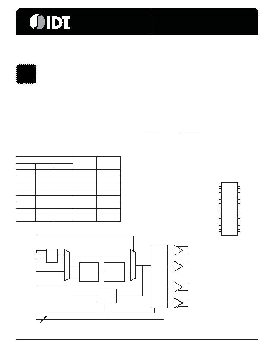
PIN ASSIGNMENT
0
1
0
Phase
Detector
VCO
÷18
÷24
÷32 (default)
÷40
N
÷1
÷2
÷3
÷4 (default)
÷8
M
OSC
3
ICS843004-02
24-Lead TSSOP
4.40mm x 7.8mm x 0.92mm
package body
G Package
Top View
nQ1
Q1
VCCo
Q0
nQ0
MR
nPLL_SEL
nc
VCCA
F_SEL0
VCC
1
2
3
4
5
6
7
8
9
10
11
12
nQ2
Q2
VCCO
Q3
nQ3
F_SEL2
nXTAL_SEL
REF_CLK
VEE
XTAL_IN
XTAL_OUT
F_SEL1
24
23
22
21
20
19
18
17
16
15
14
13
BLOCK DIAGRAM
nPLL_SEL
XTAL_IN
XTAL_OUT
REF_CLK
nXTAL_SEL
MR
F_SEL0:2
Q0
nQ0
Q1
nQ1
Q2
nQ2
Q3
nQ3
Pulldown
s
t
u
p
n
I
r
e
d
i
v
i
D
M
e
u
l
a
V
r
e
d
i
v
i
D
N
e
u
l
a
V
2
L
E
S
_
F1
L
E
S
_
F0
L
E
S
_
F
00
0
8
13
00
1
4
24
01
0
4
28
01
1
2
31
10
0
2
32
10
1
2
34
11
0
2
38
11
1
0
48
FUNCTION TABLE
发布紧急采购,3分钟左右您将得到回复。
相关PDF资料
ICS843004AGI-04LF
IC SYNTHESIZER LVPECL 24-TSSOP
ICS843021AGLFT
IC CLK GENERATOR LVPECL 8-TSSOP
ICS843022AGLF
IC CLK GENERATOR LVPECL 8-TSSOP
ICS843023AGLF
IC CLK GENERATOR LVPECL 8-TSSOP
ICS843031AG-01LF
IC CLK GENERATOR LVPECL 8-TSSOP
ICS843081AGI-01LF
IC CLK MULTIPLIER LVPECL 8-TSSOP
ICS8430AYI-61LF
IC SYNTHESIZER LVPECL 32-LQFP
ICS8430S07AKILF
IC CLK GENERATOR PLL 32VFQFN
相关代理商/技术参数
ICS843004AG-02LFT
功能描述:IC SYNTHESIZER LVPECL 24-TSSOP RoHS:是 类别:集成电路 (IC) >> 时钟/计时 - 时钟发生器,PLL,频率合成器 系列:HiPerClockS™, FemtoClock™ 标准包装:27 系列:Precision Edge® 类型:频率合成器 PLL:是 输入:PECL,晶体 输出:PECL 电路数:1 比率 - 输入:输出:1:1 差分 - 输入:输出:无/是 频率 - 最大:800MHz 除法器/乘法器:是/无 电源电压:3.135 V ~ 5.25 V 工作温度:0°C ~ 85°C 安装类型:表面贴装 封装/外壳:28-SOIC(0.295",7.50mm 宽) 供应商设备封装:28-SOIC 包装:管件
ICS843004AG-02T
制造商:ICS 制造商全称:ICS 功能描述:CRYSTAL-TO-3.3V LVPECL FREQUENCY SYNTHESIZER
ICS843004AG-125LF
功能描述:IC SYNTHESIZER LVPECL 24TSSOP RoHS:是 类别:集成电路 (IC) >> 时钟/计时 - 时钟发生器,PLL,频率合成器 系列:HiPerClockS™, FemtoClock™ 标准包装:1,000 系列:- 类型:时钟/频率合成器,扇出分配 PLL:- 输入:- 输出:- 电路数:- 比率 - 输入:输出:- 差分 - 输入:输出:- 频率 - 最大:- 除法器/乘法器:- 电源电压:- 工作温度:- 安装类型:表面贴装 封装/外壳:56-VFQFN 裸露焊盘 供应商设备封装:56-VFQFP-EP(8x8) 包装:带卷 (TR) 其它名称:844S012AKI-01LFT
ICS843004AG-125LFT
功能描述:IC SYNTHESIZER LVPECL 24TSSOP RoHS:是 类别:集成电路 (IC) >> 时钟/计时 - 时钟发生器,PLL,频率合成器 系列:HiPerClockS™, FemtoClock™ 标准包装:1,000 系列:- 类型:时钟/频率合成器,扇出分配 PLL:- 输入:- 输出:- 电路数:- 比率 - 输入:输出:- 差分 - 输入:输出:- 频率 - 最大:- 除法器/乘法器:- 电源电压:- 工作温度:- 安装类型:表面贴装 封装/外壳:56-VFQFN 裸露焊盘 供应商设备封装:56-VFQFP-EP(8x8) 包装:带卷 (TR) 其它名称:844S012AKI-01LFT
ICS843004AGI
制造商:ICS 制造商全称:ICS 功能描述:FEMTOCLOCKS-TM CRYSTAL-TO- 3.3V, 2.5V LVPECL FREQUENCY SYNTHESIZER
ICS843004AGI-01
制造商:Integrated Device Technology Inc 功能描述:IC SYNTHESIZER LVPECL 24TSSOP
ICS843004AGI-01LF
功能描述:IC SYNTHESIZER LVPECL 24-TSSOP RoHS:是 类别:集成电路 (IC) >> 时钟/计时 - 时钟发生器,PLL,频率合成器 系列:HiPerClockS™, FemtoClock™ 标准包装:27 系列:Precision Edge® 类型:频率合成器 PLL:是 输入:PECL,晶体 输出:PECL 电路数:1 比率 - 输入:输出:1:1 差分 - 输入:输出:无/是 频率 - 最大:800MHz 除法器/乘法器:是/无 电源电压:3.135 V ~ 5.25 V 工作温度:0°C ~ 85°C 安装类型:表面贴装 封装/外壳:28-SOIC(0.295",7.50mm 宽) 供应商设备封装:28-SOIC 包装:管件
ICS843004AGI-01LFT
功能描述:IC SYNTHESIZER LVPECL 24-TSSOP RoHS:是 类别:集成电路 (IC) >> 时钟/计时 - 时钟发生器,PLL,频率合成器 系列:HiPerClockS™, FemtoClock™ 标准包装:1,000 系列:- 类型:时钟/频率合成器,扇出分配 PLL:- 输入:- 输出:- 电路数:- 比率 - 输入:输出:- 差分 - 输入:输出:- 频率 - 最大:- 除法器/乘法器:- 电源电压:- 工作温度:- 安装类型:表面贴装 封装/外壳:56-VFQFN 裸露焊盘 供应商设备封装:56-VFQFP-EP(8x8) 包装:带卷 (TR) 其它名称:844S012AKI-01LFT